Silicon made possible the revolution in semiconductor miniaturization that began in the 1960s. So the fact that today size is considered a serious limitation of silicon is an indication of how far the technology has advanced since that time. As the silicon substrates used in electronics and solar cells reach their limits, how can manufacturers make components any smaller? Can graphene come to the rescue?
Graphene is a pure carbon material and the thinnest known. A layer of graphene can be only a single carbon atom thick (it takes three million layers of graphene to make a sheet 1 mm thick). Yet graphene is a staggering 200 times stronger than steel, while also being pliable. And there’s more – impermeability, transparency, together with electricity and heat conduction properties that far surpass those of silicon: graphene conducts electricity 100 times faster, and slashes the heat generation handicap of silicon based electronics.
This wonder material seems to possess only one drawback regarding its use in future nano-electronic devices. Though the best conductor of electricity, graphene does not possess a band-gap – it cannot be ‘turned off’. So a band gap has to be integrated into the material, significantly bringing its conductivity down
towards the level of silicon. Nonetheless, the performance benefits are still overwhelmingly in favor of graphene.
Graphene’s attributes create a huge potential for new and improved applications. For instance highly efficient components such as ICs and solar cells that are 100s of times thinner than they currently are; enabling transparent windows which generate electricity; bendable electronic devices, and computer chips that run on light to name a few. Furthermore, graphene can be used in the body without causing harm, opening up opportunities in the world of medicine.

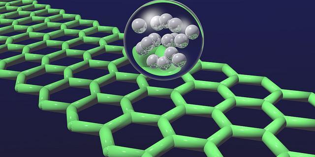
Graphene (Image Courtesy www.yaplakal.com)
We may not have long to wait for the arrival of graphene based products. Initial trials of optoelectronic devices such as touch screens and OLEDs (Organic LEDs), mobile phone batteries and composite materials for sports goods are already being carried out. However there are many technological challenges still to overcome in creating graphene ICs, and doing so at a reasonable cost.
The performance vs cost equation
The first solutions to appear will probably be in specialized areas where graphene’s performance improvements over silicon outweigh its extra cost. A similar situation is seen with other semiconductor technologies that are available, including GaAs and GaN. GaAs and GaN devices may cost more than traditional silicon but their properties – such as excellent switching speed – are invaluable in enabling systems to reach new levels of performance.
Holy grail
Graphene will not cause another electronic revolution to happen overnight. But it is on the horizon. R&D around this exciting material is intensifying, and the status of graphene research today is approaching that of silicon 50 years ago. Is history going to be repeated? But this time will the economical production of graphene electronics be the holy grail of nanomaterial researchers?


